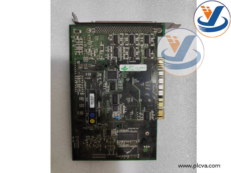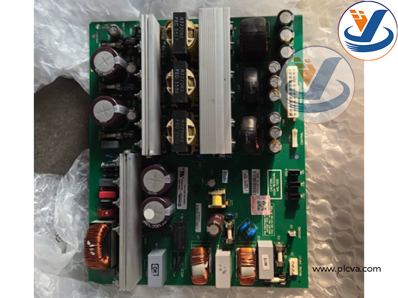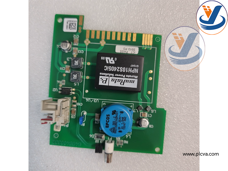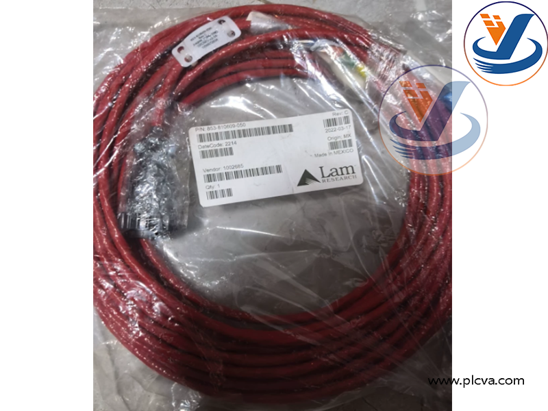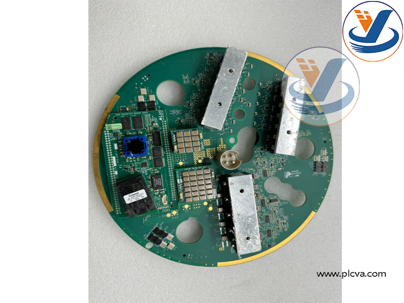
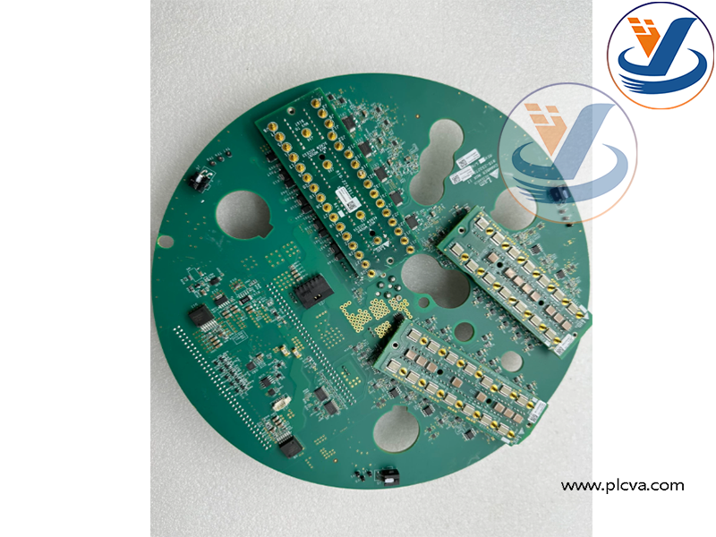
LAM Research 810‑253279‑015 Chamber Interface PCB Assembly
- Warranty: 365 days
- Quality: Original module
- Condition: New / Used
- Warehouse: Spot
- Delivery time: Shipped in 3 days after payment
- Mailbox:plcvarious@foxmail.com
Introduction
Core Functions
- Chamber‑side signal conditioning & data acquisition: Collects analog and digital sensor signals from process chamber, including temperature, pressure, gas flow, end‑point sensing and plasma‑related measurement signals. Performs signal filtering, amplification and analog‑to‑digital conversion for noisy plasma chamber environment.More products: www.plcva.com
- Bidirectional interface bridge between chamber hardware and main system controller: Translates commands from tool main controller to chamber actuators (solenoid valves, heater units, tuning components); uploads sampled process telemetry, hardware status and fault codes back to system host over internal equipment bus.
- On‑board power distribution & protection: Distributes filtered local power supply to chamber‑mounted transducers and small actuators. Implements over‑current, surge protection circuits to prevent fault propagation back to main control rack.
- Plasma‑environment noise suppression: Multi‑layer PCB ground‑plane design for high EMI immunity. Suppresses RF plasma interference generated during wafer etching process, securing stable signal quality for critical process parameters.
- Hardware fault monitoring & diagnostic feedback: Detects sensor open‑circuit, short‑circuit and power supply anomalies. Reports alarm events to tool host software for equipment interlock triggering and maintenance troubleshooting.
- Process recipe execution support: Receives recipe set‑points from main controller, executes local peripheral control sequences to support etch‑recipe steps for silicon wafer processing.

LAM Research 810‑253279‑015 Chamber Interface PCB Assembly
Applications & Use Cases
810‑253279‑015 is exclusive OEM spare component for LAM Research semiconductor wafer etch processing equipment.
- Process chamber peripheral interface unit: Mounted close to vacuum etch chamber, serves as local signal hub for chamber‑located sensors and actuators, isolating harsh chamber‑side interference from costly main control rack boards.
- Plasma etch process monitoring: Supports real‑time process data collection for dielectric and conductor etch recipes, ensures process repeatability and wafer processing yield for semiconductor fabrication.
- Equipment safety interlock participation: Delivers chamber hardware status signals to main controller, participates in safety interlock logic, prevents wafer scrap and hardware damage under abnormal chamber conditions.
- Reduction of long‑distance signal degradation: Handles signal conditioning locally near chamber, minimizing analog signal drift and noise corruption from long cable runs between chamber and control cabinet.
- Fab equipment maintenance & spare‑part replacement: Used for field swap of defective chamber‑interface PCBs on legacy LAM etch production tools. Extends system service life without redesigning the whole chamber control architecture.plcva.com

LAM Research 810‑253279‑015 Chamber Interface PCB Assembly
| Understand the lowest price, please contact via email: plcvarious@foxmail.com |
| More products: www.plcva.com |
| Many products are not yet on the shelves please contact us for more products. |