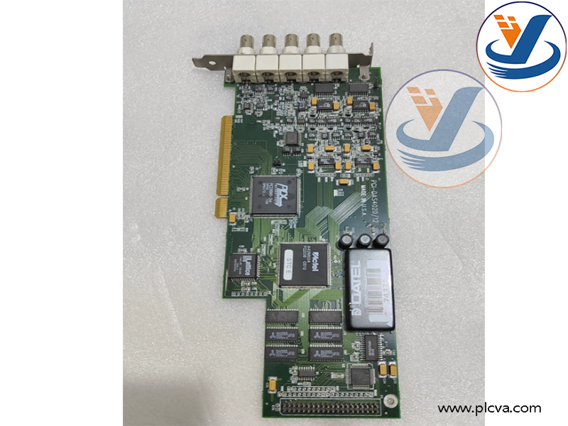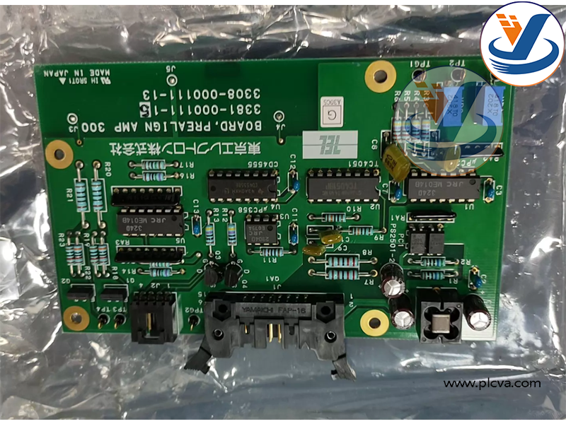
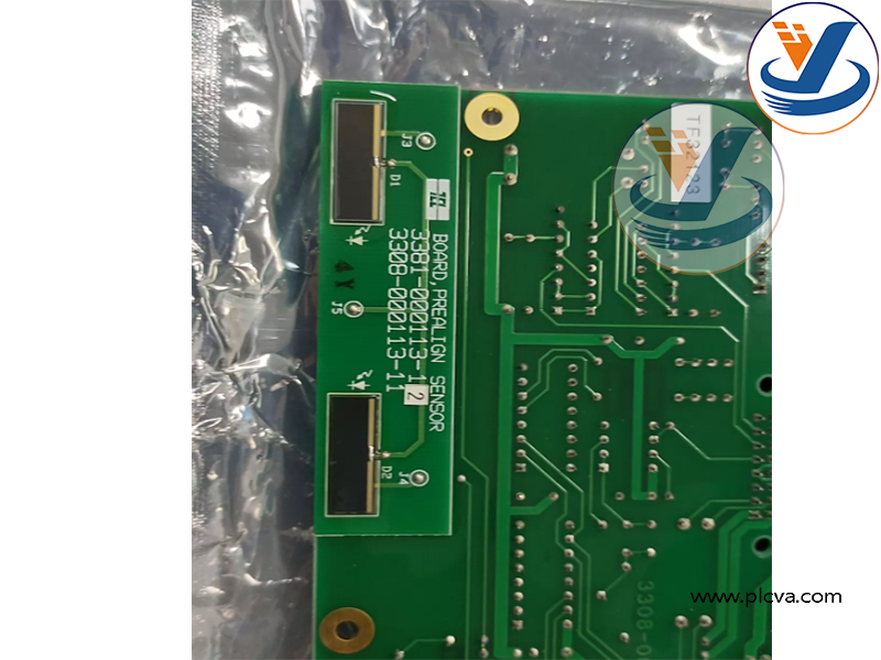
TEL Tokyo Electron 3381‑00011‑15 / 3308‑000111‑13 Prealign‑AMP Board PCB
- Warranty: 365 days
- Quality: Original module
- Condition: New / Used
- Warehouse: Spot
- Delivery time: Shipped in 3 days after payment
- Mailbox:plcvarious@foxmail.com
Introduction
Core Functions
- Optical sensor signal amplification & conditioning: Receives weak analog signals from the pre‑aligner optical photo‑sensors (edge notch / flat‑find sensors for silicon wafer). Amplifies, filters and denoises tiny photocurrent signals, converts them into stable analog voltage signals for backend digital acquisition circuit.More products: www.plcva.com
- Wafer notch / flat edge detection signal processing: Processes optical feedback signals for wafer pre‑alignment. Detects wafer notch or flat orientation mark, provides high‑quality signal source for calculating wafer rotational position and offset angle.
- Signal isolation and noise suppression: Suppresses electromagnetic interference generated by robot motors, vacuum pumps and plasma‑related modules inside semiconductor tool. Guarantees stable signal quality in high‑EMI factory cabinet environment.
- Bidirectional signal bridge: Transmits conditioned alignment measurement signals to equipment main control CPU; receives reference voltage and power supply from system control rack, provides regulated power for pre‑aligner optical sensor heads.
- Hardware fault detection: Monitors sensor signal amplitude and board operating status. Reports sensor disconnection, signal abnormality and board hardware failure to tool host, triggers alarm for maintenance troubleshooting.
- Stable analog reference output: Provides precise reference bias voltage for pre‑align optical sensors, ensuring consistent detection threshold for wafer edge/notch detection across long‑term production runs.

Applications & Use Cases
This is exclusive OEM spare‑part for TEL 300 mm Clean‑Track Coater‑Developer photoresist processing equipment, installed in the wafer pre‑aligner station of wafer handling subsystem.
- Wafer pre‑alignment station core signal processing: Processes optical sensor signals for pre‑align unit. Detects wafer notch/flat feature, calculates wafer rotation offset, completes coarse orientation correction before wafer is transferred to process chamber. Accurate pre‑alignment is critical for photoresist coating, exposure and developing process accuracy.
- Semiconductor photolithography process preparation: Ensures correct angular orientation of 300 mm silicon wafers prior to spin‑coating, developing and lithography exposure steps, prevents mis‑alignment‑caused wafer scrap.plcva.com
- Wafer robot handling coordination: Cooperates with wafer transfer robot. Delivers alignment offset data to motion control unit, helping robot place wafer with correct angle into process chuck.
- Process stability guarantee: Reduces signal drift and noise interference, improves pre‑align repeatability, supports high‑volume fab mass production yield.
- Equipment maintenance & spare‑part replacement: Used as field‑swap spare for defective prealign‑amp boards on legacy TEL Clean‑Track tools. Extends equipment service life without redesigning wafer handling subsystem.

| Understand the lowest price, please contact via email: plcvarious@foxmail.com |
| More products: www.plcva.com |
| Many products are not yet on the shelves please contact us for more products. |